|
Pulsed-laser ablation
: thin films
Supported by :

|
|
Description
We are using a pulsed-laser ablation deposition (PLD) system to prepare
high quality thin films which are used in a wide series of studies exploring
the most fundamental questions as the mechanism of high temperature superconductivity,
but also designing new devices on various lengthscales. These high quality
films will be used for fundamental and applied research, a major part within
the infrastructure already in place at the QML and IMSI (in particular
the equipment used for nanolithography at the Electrical Engineering Dept
at the Université de Sherbrooke), but also through external collaborations.
Pulsed laser deposition has been under strong development since the
discovery of high temperature superconductors. This technique is now used
in the fabrication and study of oxide-based devices, for example the spin-polarized
injection devices composed of superconducting (YBCO) and ferromagnetic
(LSMO) components. In our group, we use for example PLD for optimisation
of composition of the electron-doped cuprates. Since they possess a very
narrow range of Ce concentrations exhibiting superconductivity (Tc
is peaked around x = 0.15), it makes them more sensitive to inhomogeneities
than the hole-doped cuprates. To study their physical properties, we use
PLD to target a very accurate cerium content. It is then possible to get
c-axis oriented thin films even in the concentration range from x = 0.12
to x = 0.15 where Tc goes from 0 to 22K (in PCCO).
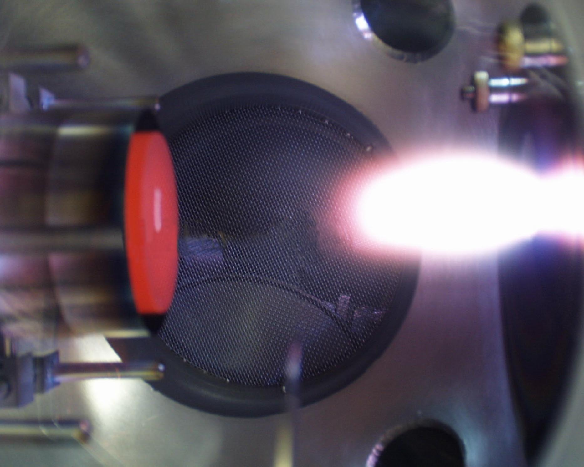
Principle of operation
A target made of polycrystalline materials (most often with the desired
stoichiometry) is hit by a high energy pulsed laser beam (KrF excimer laser
: typical energy density at the target of 2 J/cm2 with typical
repetition rate of 5 to 10 Hz). Materials is ablated from the target, and
sputtered toward a hot substrates. The various ions, with high energy and
high mobilities for such high temperatures, deposit on the substrate and
form the desired crystal structure, after optimisation of several parameters
: temperature, nature and position of substrate, type of atmosphere and
its pressure during deposition, energy density of laser, post-annealing
treatments (time and type),... The final goal, usually, is to obtain epitaxial
thin films, having preferred orientation and most of their properties very
close to the bulk (crystalline) ones. This is achieved after a complete
exploration of the abovementoned growth parameters. A very active area
at the present time is the exploration of the effect of artificial pressure
(from the substrate) onto the properties of the materials deposited.
 PLD system (U.
de Sherbrooke)
PLD system (U.
de Sherbrooke)
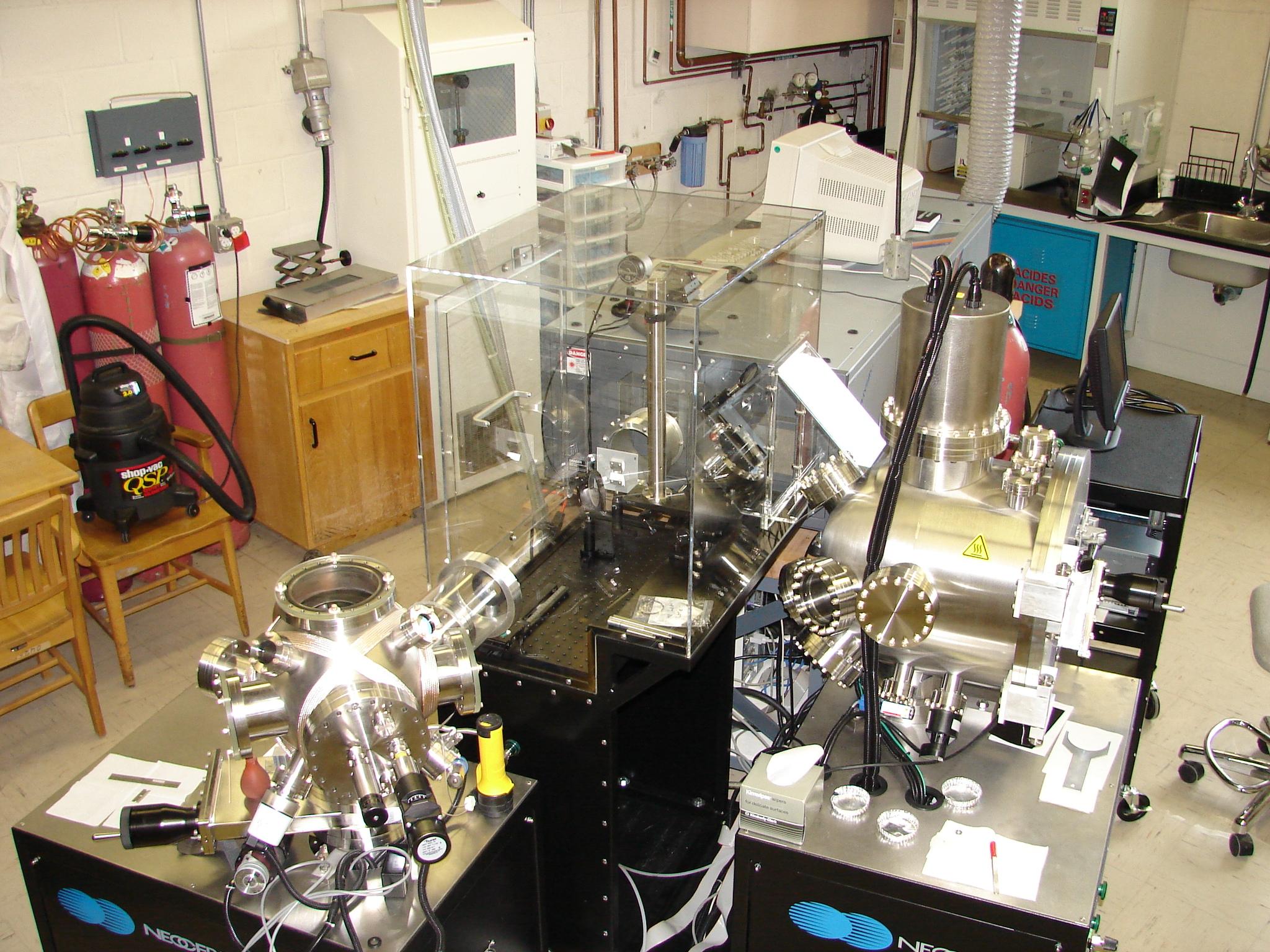
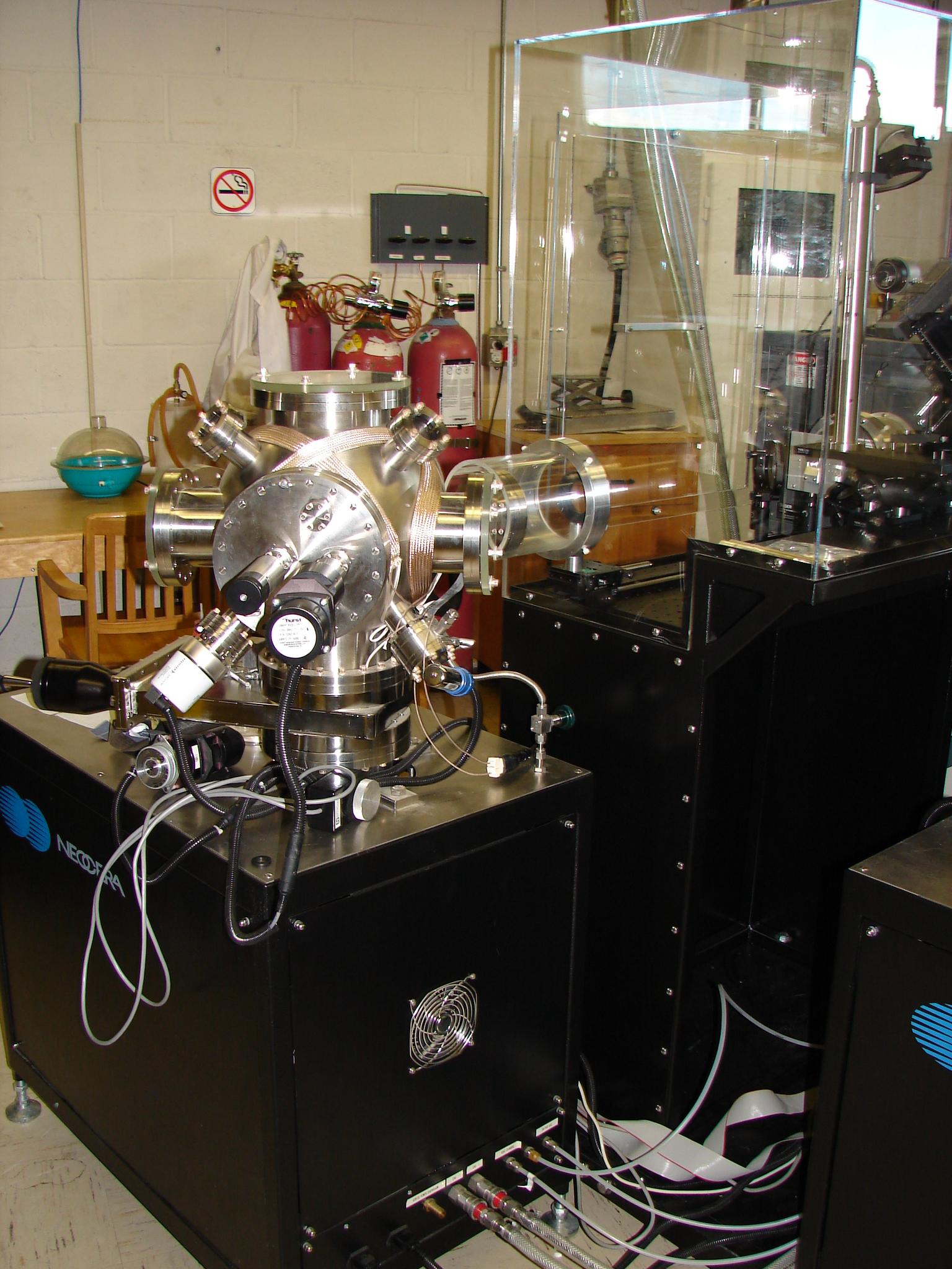
Our laboratory
Our thin film growth laboratory includes :
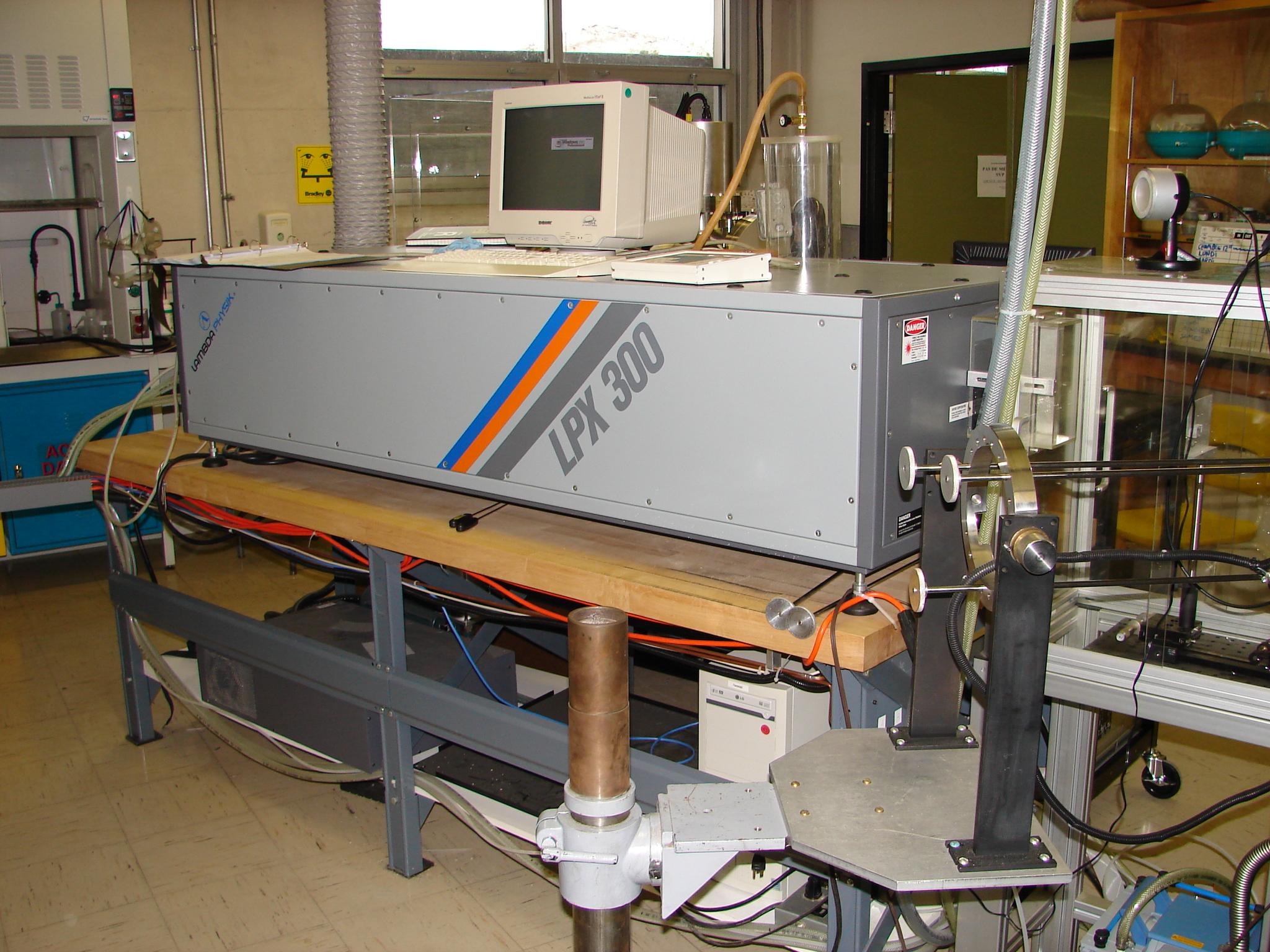
1) A pulsed laser from Lambda Physik (LPX 305)
Maximum energy per pulse : 1.4 J
Pulse width : 20 ns
Maximum repetition rate : 50 Hz
|
|
2) A conventional 12" diameter spherical chamber (Neocera)
Max substrate temperature : 950oC
Gas : O2, N2O, Ar
Max Substrate size : 1 cm2
|
|
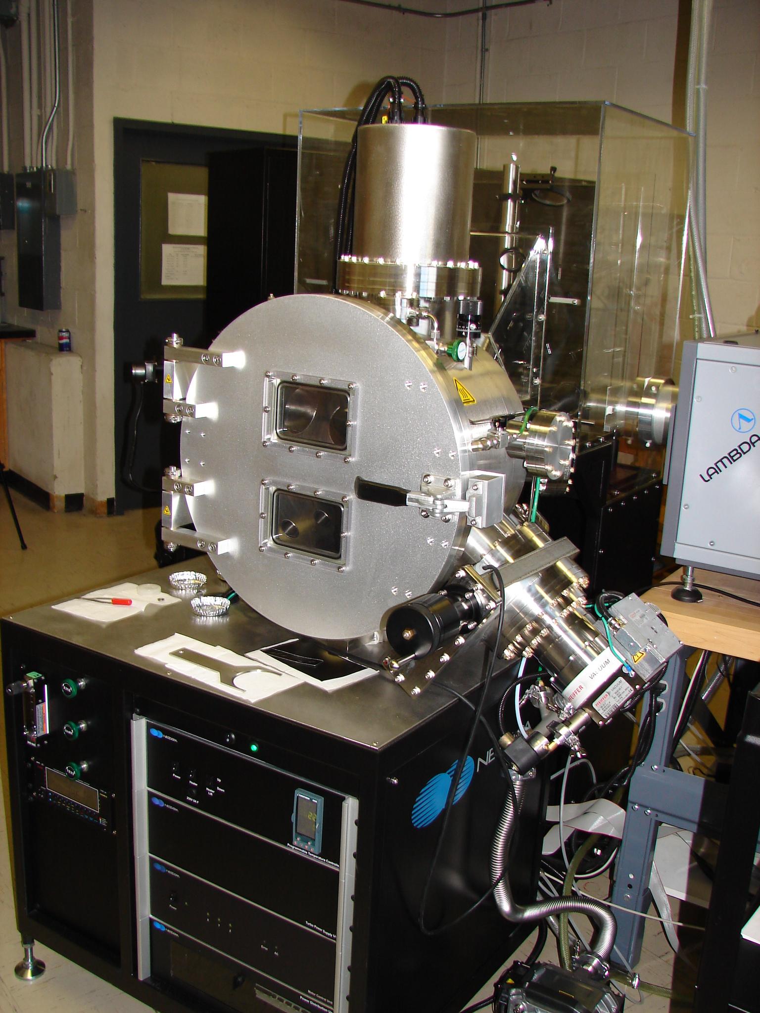
3) A custom 18" diameter semi-spherical chamber with hinged front
door (Neocera)
Max substrate temperature : 950oC
Gas : O2, N2O, Ar
Max Substrate size : ~3x3 cm2 (2" diameter)
|
|
This laboratory is part of the Réseau québécois
sur les matériaux de pointe (RQMP)
, the Quantum Materials Laboratory (QML) and the Institut des
matériaux et systèmes intelligents (IMSI).
Last modified : 30 March 2006 (P.F.)